

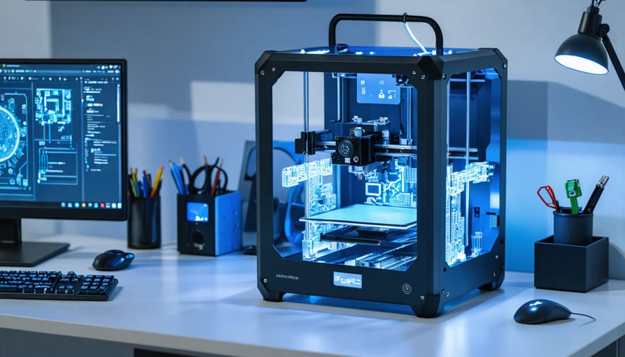
3D-printed electronics represent a revolutionary convergence of additive manufacturing and circuit design, enabling makers to create custom PCBs, sensors, and interactive devices directly from their desktop. By combining conductive filaments with traditional 3D printing materials, innovators can now fabricate complex electronic components that were previously impossible or prohibitively expensive to produce through conventional manufacturing methods.
This emerging technology has transformed prototyping and small-scale production, allowing makers to iterate designs rapidly and embed electronics directly within printed structures. From functional antennas and capacitive touch sensors to complete circuit housings with integrated conductivity, 3D-printed electronics offer unprecedented freedom in designing custom electronic solutions.
The real power of this technology lies in its accessibility and versatility. Whether you’re developing IoT devices, wearable technology, or custom robotics, 3D-printed electronics provide the tools to bridge the gap between mechanical design and electrical functionality. With multi-material printers becoming more affordable and conductive materials more reliable, makers can now prototype complete electronic devices in hours rather than weeks.
For hobbyists and professionals alike, mastering 3D-printed electronics opens up new possibilities in custom device creation, rapid prototyping, and innovative problem-solving. This guide will explore the essential techniques, materials, and best practices for successfully integrating electronics into your 3D printing projects.
How 3D Printed Electronics Actually Work
Conductive Materials and Filaments
Conductive materials for 3D printing electronics have evolved significantly, offering makers various options for creating functional circuits. The most common materials include conductive PLA, which combines traditional PLA with carbon particles or metal powders, and specialized silver-based conductive inks. These materials typically require careful post-processing your printed circuits to achieve optimal conductivity.
Popular choices include Proto-pasta’s Conductive PLA, with a resistance of approximately 30 ohms/cm, and Multi3D’s Electrifi filament, which offers better conductivity but requires lower printing temperatures. Some manufacturers also produce copper and graphene-infused filaments, which balance conductivity with ease of use.
When selecting materials, consider both conductivity requirements and printing characteristics. Many environmentally friendly filaments now include conductive properties, making them suitable for basic electronic projects. For high-performance applications, dual-extrusion printing combining conductive and insulating materials offers the best results, enabling complex circuit designs within a single print.
Multi-Material Printing Techniques
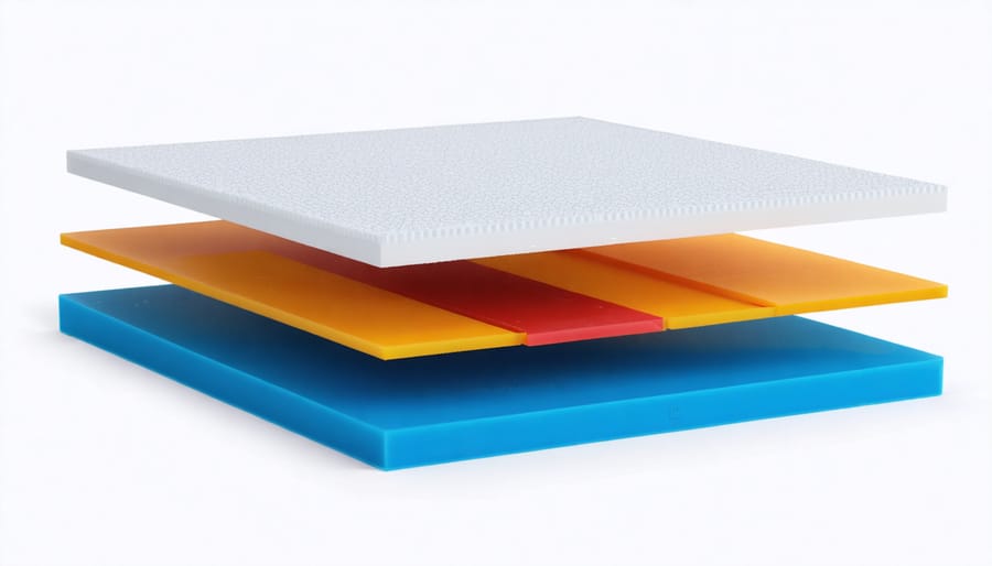
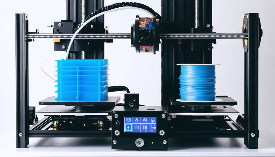
Multi-material 3D printing for electronics requires sophisticated techniques to combine conductive and non-conductive materials effectively. The most common method involves dual-extruder setups, where one extruder handles standard thermoplastics like PLA or ABS, while the second manages conductive materials such as silver-based inks or carbon-infused filaments.
Layer-by-layer deposition is crucial for creating functional electronic components. The printer first lays down the base structure using non-conductive material, then switches to conductive filament for circuit traces and connection points. Some advanced systems use specialized tool-changing mechanisms to seamlessly alternate between multiple materials without contamination.
Recent innovations include direct-write technology, which enables the precise placement of conductive inks using micro-dispensing nozzles. This method allows for intricate circuit patterns and higher resolution than traditional FDM printing. Manufacturers also employ hybrid systems that combine traditional 3D printing with pick-and-place mechanisms for embedding pre-made electronic components during the printing process.
For best results, careful consideration of material compatibility and printing temperatures is essential, as different materials often require specific printing conditions to achieve optimal conductivity and adhesion.
Essential Equipment for Electronics 3D Printing
Printer Requirements and Modifications
3D printing electronics requires specialized printer features and modifications beyond standard FDM setups. The printer must support multiple extruders or tool heads to handle different materials, including conductive filaments and insulators. A heated bed is essential, typically capable of reaching temperatures between 60-110°C for proper adhesion of electronic materials.
Print head precision is crucial, with recommended layer heights of 0.1mm or less for intricate circuit patterns. The printer should have a robust cooling system, with maintaining proper cooling being particularly important when working with temperature-sensitive electronic components.
Common modifications include installing a direct-drive extruder for better control over conductive materials, upgrading to a hardened steel nozzle to prevent wear from abrasive materials, and adding a sealed enclosure to maintain consistent printing temperatures. Some makers also add automatic bed leveling systems for enhanced first-layer accuracy.
For safety considerations, the printer should feature thermal runaway protection and proper electrical grounding. Adding a HEPA filter system is recommended when printing with conductive materials to manage potentially harmful particles. The build surface should be compatible with both standard filaments and specialized electronic materials, with removable spring steel sheets being a popular choice.
Software Tools and Design Considerations
Creating 3D-printed electronics requires specific software tools and careful design considerations to ensure successful prints and functional electronic integration. For design work, CAD (Computer-Aided Design) software like Fusion 360, TinkerCAD, or FreeCAD offers the necessary features for creating enclosures and component holders. These programs allow you to design precise measurements for electronic components while maintaining proper clearances and support structures.
For slicing your 3D models, popular options include Cura, PrusaSlicer, or Simplify3D. When configuring your slicer settings, pay special attention to infill density, wall thickness, and support structures, as these directly impact the structural integrity of your electronic enclosures.
Key design considerations include:
– Planning for heat dissipation with adequate ventilation holes
– Incorporating cable management features
– Designing snap-fit closures for easy access
– Including mounting points for circuit boards and components
– Considering layer orientation for maximum strength
When designing multi-material prints for conductive elements, specialized software like Voxel8 can help manage different material properties and printing parameters. Always verify your dimensions with test prints before committing to full projects, and maintain proper tolerances for electronic components (typically 0.2-0.4mm clearance).
Remember to export your files in the appropriate format, usually .STL or .3MF, and validate your models for any mesh errors before printing.
Practical Applications with Raspberry Pi
Custom Sensor Housing Projects
Creating custom sensor housings with integrated circuits is a rewarding project that combines 3D printing and electronics in a practical way. Start by designing your housing in a 3D modeling program, ensuring adequate space for your sensor components and necessary ventilation. Include mounting points for circuit boards and cable management features to keep everything organized.
When designing your housing, consider creating a two-part shell that snaps together, making it easier to access and maintain the electronics inside. Add internal supports and standoffs to keep circuit boards elevated and properly positioned. Remember to include cutouts for sensor exposure, power cables, and any necessary interface connections.
For weather-resistant projects, incorporate seal channels and gasket spaces into your design. Use PETG or ABS filament for better durability and heat resistance compared to standard PLA. Consider printing with a higher infill percentage (40-60%) in areas that need extra structural support.
Include these essential features in your sensor housing design:
– Mounting brackets or screw holes for secure installation
– Cable strain relief to protect connections
– Alignment pins for precise assembly
– Ventilation holes or grills for heat dissipation
– Access ports for firmware updates or maintenance
Before printing, test-fit your components using a prototype printed at a lower resolution. This saves time and material while allowing you to make necessary adjustments. Once satisfied with the fit, print the final version at higher quality settings (0.2mm layer height or finer) for a professional finish.
Finally, when assembling your sensor housing, use heat-set inserts for stronger threaded connections and consider adding silica gel packets for moisture protection in outdoor applications.
3D Printed GPIO Extensions
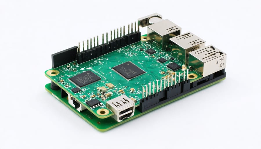
Creating custom GPIO extensions through 3D printing opens up endless possibilities for Raspberry Pi projects. Whether you need a specific sensor mount, a custom case with GPIO breakouts, or a specialized interface board holder, 3D printing provides the flexibility to design exactly what you need.
To design your GPIO extensions, start by measuring the standard GPIO header dimensions (2.54mm pitch) and creating a basic model in your preferred CAD software. Programs like FreeCAD or Tinkercad work well for beginners, while advanced users might prefer Fusion 360. Ensure your design includes proper pin spacing and alignment features to prevent misconnection.
When printing GPIO extensions, use a material with good dimensional stability like PETG or ABS. PLA can work for simple projects, but it may deform under heat from electronic components. Print with a layer height of 0.2mm or less for smooth pin holes, and consider using a 0.4mm nozzle for precise details.
Popular GPIO extension designs include:
– Stacking headers with extended pins
– Angled breakout boards for tight spaces
– Custom sensor mounts with integrated wire channels
– Project-specific interface panels
Always test-fit your printed parts with header pins before soldering any components. Include alignment guides and support structures in your design to ensure proper fit and prevent stress on the GPIO pins. For better durability, consider adding reinforcement ribs and mounting points to your designs.
Remember to maintain proper clearance for heat dissipation and include ventilation holes if your extension will be enclosed. This prevents potential damage to both your Raspberry Pi and attached components.
Troubleshooting Common Issues
Print Quality Problems
When 3D printing electronic components and enclosures, several common quality issues can affect the final result. Layer adhesion problems are particularly critical when printing cases for electronic components, as they can compromise structural integrity and protection. To prevent this, ensure your print bed is properly leveled and maintain optimal printing temperatures for your chosen filament.
Warping is another significant concern, especially when printing larger enclosures for electronic projects. This can cause misalignment of mounting holes and prevent components from fitting correctly. Using a heated build plate and applying appropriate bed adhesion solutions can help minimize warping issues.
Stringing between parts can interfere with electronic component placement and create short circuit risks. Adjust your retraction settings and printing temperature to reduce stringing. For precision-critical elements like PCB mounts or connector housings, ensure your printer’s calibration is spot-on and consider using a smaller nozzle size for enhanced detail.
Watch out for overhanging features, which are common in electronic enclosure designs. Poor overhangs can affect cooling vents and cable management channels. Using proper cooling settings and strategic support placement will help maintain the structural integrity of these features. Regular maintenance of your printer, including checking for worn nozzles and loose belts, is essential for consistent quality in electronics-related prints.
Conductivity Challenges
One of the biggest challenges in 3D printing electronics is achieving reliable electrical conductivity. While traditional PCBs offer excellent conductivity through copper traces, 3D printed circuits face several hurdles. The most common issue is the limited conductivity of printable materials, even those marketed as conductive filaments. These materials often have higher resistance compared to traditional copper conductors, which can affect signal integrity and power delivery.
Temperature management presents another significant challenge. Many conductive materials require specific printing temperatures that might not align well with the base material’s requirements. This can lead to poor layer adhesion or inconsistent conductivity throughout the printed circuit. Additionally, the thermal expansion rates between conductive and non-conductive materials can cause stress points or breaks in the electrical pathways during use.
Surface finish and contact resistance also play crucial roles. Printed conductive traces often have rough surfaces, which can lead to poor connections with components and increased contact resistance. This is particularly problematic when connecting traditional electronic components to 3D printed circuits.
To overcome these challenges, makers often employ hybrid approaches, combining 3D printed structures with traditional electronic elements. This might include embedding copper wire into printed channels, using conductive paint, or creating slots for PCB insertion. While these solutions add complexity to the design process, they often result in more reliable electronic builds.
The future of 3D printed electronics stands at an exciting crossroads, where innovation meets accessibility. As technology continues to advance, we’re seeing remarkable improvements in both printing materials and techniques, opening up new possibilities for makers and innovators alike. The ability to create custom circuit boards, embedded sensors, and functional electronic components directly through 3D printing is revolutionizing how we approach electronic device manufacturing.
Looking ahead, we can expect to see even more sophisticated applications, from printable batteries and flexible displays to fully integrated smart devices. The democratization of electronics manufacturing through 3D printing is particularly promising for rapid prototyping and small-scale production, making it easier than ever for hobbyists and small businesses to bring their ideas to life.
The integration of artificial intelligence and machine learning into 3D printing software is also set to streamline the design process, automatically optimizing circuit layouts and component placement. This advancement, combined with increasingly affordable and user-friendly 3D printers, suggests a future where creating custom electronic devices could be as commonplace as printing documents today.
For the maker community, this means unprecedented opportunities to experiment with new designs and create innovative solutions to everyday problems. Whether you’re a hobbyist working on your next project or an educator teaching the next generation of inventors, 3D printed electronics offers a powerful platform for turning creative ideas into reality.